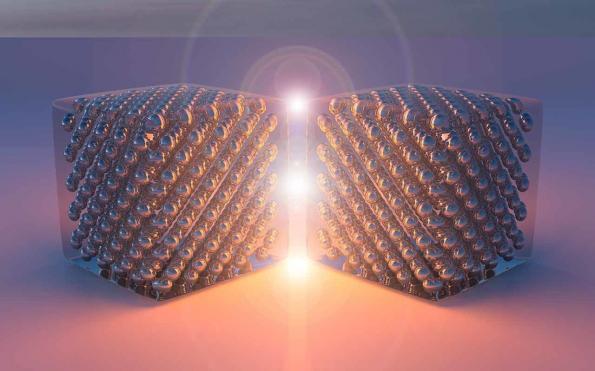
The bow-tie-shaped plasmonic nanostructure described in a paper titled "Efficient light generation from enhanced inelastic electron tunnelling" published in Nature Photonics consists of two single crystals silver cuboids joined at one corner, yet separated by a 1.5nm thin insulating polymer (PolyVinylPyrrolidone or PVP). Applying a voltage across the tiny junction allows electrons to tunnel from one corner to the next through the PVP barrier, transferring some of their energy to surface plasmon polaritons along the metal-insulator interface which then radiate that energy into photons.
The extremely small feature sizes and specific geometry of the junction make it particularly efficient at tunnelling electrons inelastically, meaning more energy can be transferred from the tunnelling electrons to the plasmon polaritons.
Read more HERE
![]() C/ Sèquia de Benàger 23
C/ Sèquia de Benàger 23
Pol. Ind. Alquería de Moret
46210 Picanya (Valencia) Spain